

2026-03-08
High-voltage nanosecond pulse converter
Short, high-voltage pulses of nanosecond duration are widely used in scientific and instrumentation, where the generation of high-amplitude electrical signals with very short rise times is required. Such pulses are used to control optical modulators and Pockels cells, to gate microchannel plates in high-speed detectors and cameras, in ultra-wideband radar systems, as well as in experiments in plasma physics, scalar fields, free energy, laser diagnostics, and biophysical research. All these applications require a source of pulses with steep rise times and amplitudes on the order of kilovolts and durations of a few nanoseconds.
The purpose of this device is to convert low-voltage rectangular pulses of relatively low frequency into high-voltage pulses of nanosecond duration. The device is based on the circuit described in [1], but the proposed implementation has a number of distinctive circuit and design features.
The device input receives rectangular pulses with an amplitude of approximately 12 V and a repetition rate of 1 Hz - 10 kHz. At the device output, with a 75 ohm load, pulses with an amplitude of approximately 1 kV or higher, a duration of approximately 4 ns, and a rise and fall time of approximately 2 ns are generated. The converter requires a +3 kV power source, which is generated by multiplying the industrial line voltage. The parameters of the presented device are approximately an order of magnitude superior to those of a line-powered avalanche pulse generator and provide pulse rise and fall rates of up to 500 V/ns or more.
One possible application for this converter is presented here.
Circuit Operation
The circuit in Figure 1 is an ultrashort high-voltage pulse generator that uses a series cascade of nine bipolar transistors (U1-U9) operating in avalanche breakdown mode. The transistors are connected in series and powered by a high-voltage source of approximately three kilovolts. To evenly distribute the voltage between them, a resistive network R1-R9 is used, allowing each transistor to hold only a portion of the total voltage. While the device is in standby mode, all transistors are off, and the network is at high voltage, effectively acting as a high-voltage switch ready to operate.
The device is activated by a short trigger pulse, which is applied to transistor U9 through pulse transformer TI1. Under the influence of this pulse, the first transistor enters avalanche breakdown, which causes a sharp drop in voltage across it and redistributes the voltage across the remaining elements of the cascade. As a result, the voltage across subsequent transistors exceeds their avalanche breakdown threshold, and they also sequentially enter avalanche mode. This process develops very quickly and leads to the almost simultaneous activation of the entire transistor chain.
 Fig. 1. Schematic diagram of the nanosecond high-voltage pulse converter |
When the entire cascade is in a conducting state, the accumulated energy of the high-voltage source is quickly discharged through capacitor C1-C2 to the load (not shown in diagram 1), generating a short high-voltage pulse. Due to the avalanche mode of the transistors and the low parasitic parameters of the design, the pulse has a very short duration and a steep rise time, which allows voltages of approximately a kilovolt to be obtained with pulse durations of several nanoseconds.
With sequential avalanche triggering of the transistors, the total switching time is significantly shorter than the switching time of a single transistor.
Component Base
The TI1 pulse transformer can be manufactured in various ways, or a ready-made transformer with suitable parameters can be used. The following condition must be met during its manufacture: the ratio of the number of turns of the primary winding to the number of turns of the secondary winding must be equal to the ratio of the pulse amplitude of the master oscillator to a voltage of 6 V—the VEBO value of transistor U1.
The author's design for the TI1 transformer uses a ferrite core measuring 16×10×4.5 mm with a magnetic permeability of about 2000 (Material: 2000NM). The primary winding contains 8 turns, the secondary winding contains 4 turns. This ratio is chosen based on the fact that the master oscillator generates pulses with an amplitude of approximately 12 V. Ferrite rings of other sizes and materials with different magnetic permeability may be used, provided the required transformation ratio is maintained.
A few words about the resistor R11 should be said. This should be a high-voltage resistor with a power rating of at least 5 W, such as HVR40AH. If the master oscillator frequency is less than 3 kHz, then installing one such resistor on the printed circuit board will be sufficient. But if the pulse repetition rate is expected to be higher, another resistor of the same value must be installed in parallel. On the printed circuit board, it is indicated as R12.
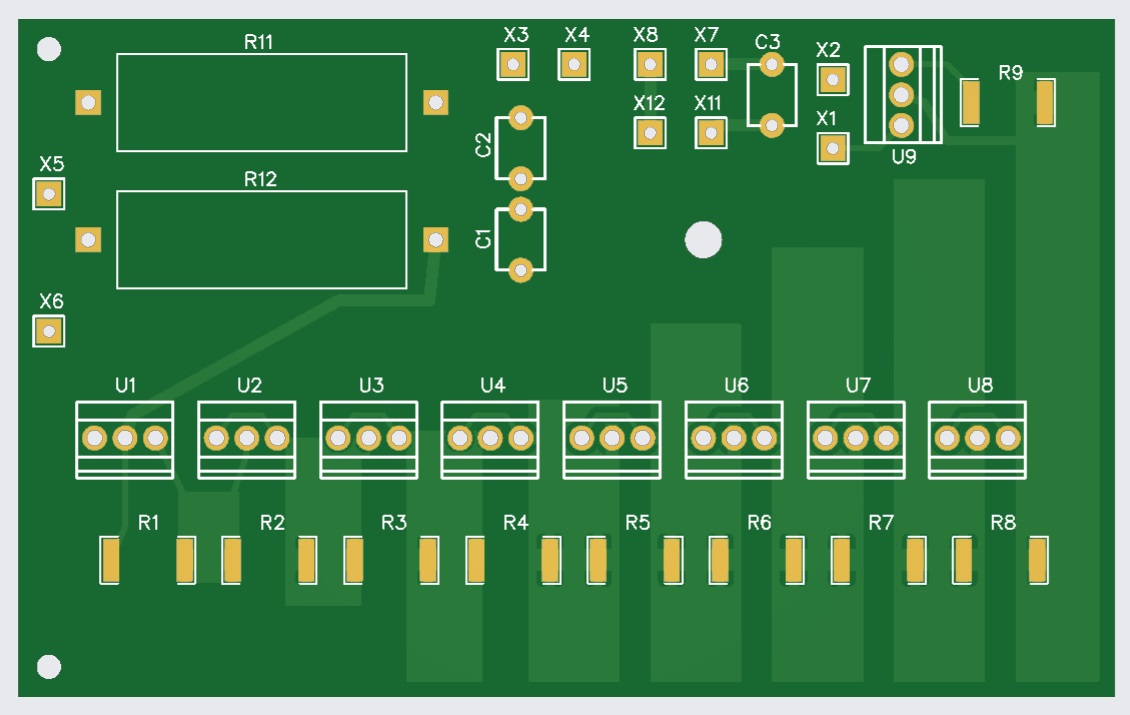
 Fig. 2. External view of the nanosecond high-voltage pulse converter board | 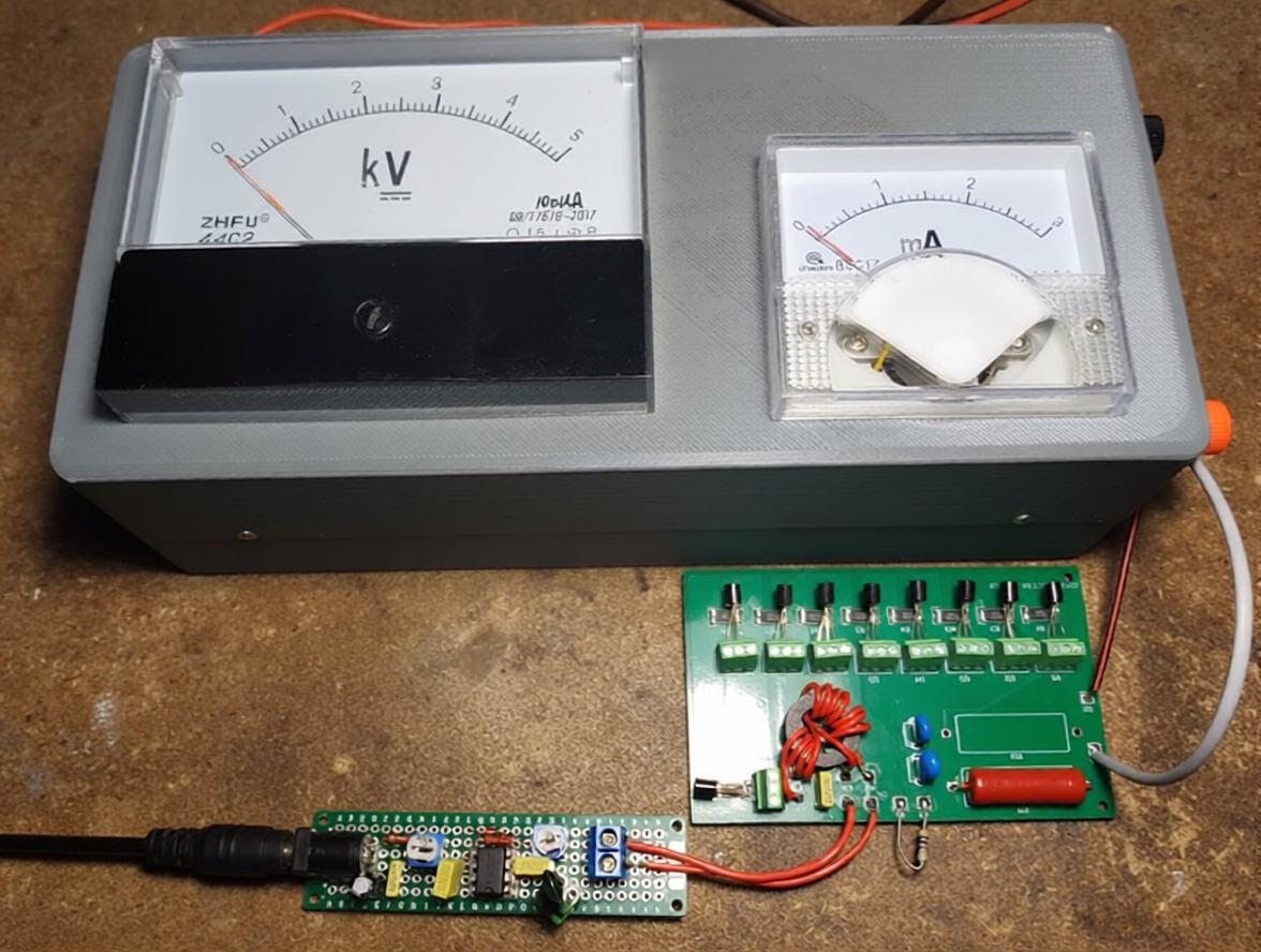 Fig. 3. Connection of blocks for measuring nanosecond high-voltage pulses |
Capacitors CP1-CP8 change their capacitance stepwise from 0.9 picofarads (CP1) to 9.2 picofarads (CP8). They are implemented directly on the board by creating a capacitance between the tracks of double-sided fiberglass, 1.6 mm thick (FR-4).
Capacitors C1-C2 are ceramic. There are two options: install two 30 pF capacitors in series on the board, each rated for 2 kV, or a single 15 pF capacitor rated for 4 kV. Capacitor C3 can be any non-electrolytic.
Transistors U1-U9 use 2N5551. You can try using other similar ones. It is preferable that they all be from the same batch. The author additionally installed sockets under each transistor to allow for quick replacement, but this turned out to be unnecessary.
Connecting Blocks
To generate high-voltage pulses of nanosecond duration, two more functional blocks must be connected to the converter circuit (Fig. 1). The entire block diagram is shown in Figure 4.
1) Rectangular Pulse Generator – Master Oscillator. In Block Diagram 4, it is designated as G1. Its function is to generate rectangular pulses at the output, which trigger the transistor cascade of the GIHV converter. For this generator, the author used a classic NE555 circuit, which can be quickly assembled from simple components on a circuit board. However, any other rectangular pulse source with suitable parameters can be used instead. The pulse repetition rate must match the required high-voltage pulse repetition rate at the device's output and is typically in the range of several kilohertz. The generator is galvanically isolated from the main converter circuit, thereby eliminating any possible impact of high-voltage pulses on its electronic components.
 Fig. 4. Block diagram of block connections and measurement of nanosecond high-voltage pulses |
2) High voltage source. In the block diagram, it is designated as PHV. This block supplies the converter circuit with the required constant high voltage, which generates high-amplitude output pulses. The author used a ready-made multiplier circuit for this unit for a 3 kV line voltage. It requires connecting a LATR—a transformer with an adjustable output voltage of 0..220 V. It is designated as TRL in the block diagram.
A 75-ohm active resistor R1 must also be connected to the output of the GIHV converter. And then connect the oscilloscope probe OS1 to it.
Photo of the device assembled by the authorThe design can be seen in Figure 3.
Starting the Device and Measurements
First, the master oscillator G1 is started (Fig. 4). Then, the LATR TRL network transformer is turned on, and by turning its knob, its output voltage is gradually increased, fed to the voltage multiplier PHV. Meanwhile, the output of the nanosecond high-voltage pulse converter GIHV, connected to the active resistance R1, is monitored by the oscilloscope OS1. When the first pulses appear, turn the TRL knob a little further until a stable sequence is achieved.
The author's measurements were performed with an OS1 oscilloscope (RIGOL DS1202) using a high-voltage probe with a 1:100 division ratio, rated for voltages up to 2 kV. The oscilloscope's rated bandwidth is 200 MHz; in practice, the device is capable of recording signals up to frequencies of approximately 300 MHz. However, even this frequency range is insufficient to accurately determine the rise and fall times of the pulse at the device's output. According to oscilloscope measurements, the rise and fall times are approximately 2 ns. It should be noted that the actual duration may be shorter—down to ~1 ns—but the limited bandwidth of the measurement path prevents reliable measurement.
 Fig.5. Resolution 5 ns/cell |  Fig.6. Resolution 20 ns/cell |  Fig. 7. Resolution 200 µs/cell |
The waveforms obtained in this way can be seen in Figures 5-7. Photo 5 shows a high-voltage nanosecond pulse measured at the circuit output, across a 75 ohm load. Photo 7 shows a series of such pulses, repeated at the frequency of the master oscillator.
Printed Circuit Board
This design option has been well-developed by the author. It adheres to all the necessary dimensions to achieve the correct capacitance values CP1-CP8, achieved by specifying specific areas between the double-sided fiberglass traces.
Production version: PCB (open)
The production option provides a set of documentation for manufacturing a printed circuit board in production:
GERBER file for PCB, BOM file of the specification of components and a schematic diagram showing the values of the elements.
All this allows you to immediately order a PCB, for example, here, and then quickly assemble it.
 |  |
When ordering, be sure to select the board material: 1.6 mm thick fiberglass, grade FR-4.
Materials used
- Manohar Lal Sharma. High voltage picosecond pulse generation by an avalanche transistor stack on microstrip PCB. [PDF]